Sie erhalten in Kürze eine Bestätigung per E-Mail.
Tuesday | 04/10/2022 | 11:00 am
Due to the component shortage in electronic industry and the dependency on Asian suppliers, the European Community decided to double Europe’s global market share in Semi-Conductor industry to 20% in 2030. This requires huge investments in new production and research capacities. To achieve this goal, the EU launched at the 8th of February 2022 “The European Chips Act”, which will mobilise €43 billion Euros of public and private investments.
At the same time, we see a trend to a multi-chip packaging process. Moore’s Law is not valid anymore. The effort to develop smaller structures is too high, but the opportunities and benefits in combining different chips and components in one package are promising. Complex functions of whole devices can be integrated into a small BGA or IC package. This trend affects all packaging processes from 2D via 3D down to wafer-level packaging.
The packaging process is getting more complex and challenging, but new interconnection methods like hybrid-bonding and interposer materials allowing a higher density and integration level. Smaller components, higher density and new materials are challenging the existing inspection and measurement systems. Tailored measurement devices are required to support the new packaging trends. Especially, when the boundaries between front-end and back-end applications or back-end and SMT are blurring.
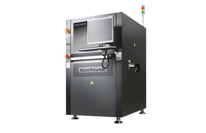
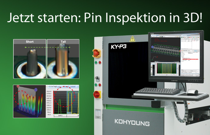
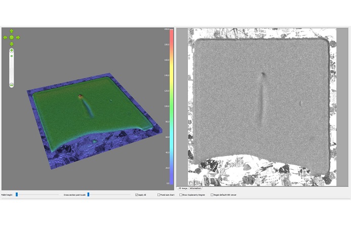
3D Moiré Interferometry measurement is the recent standard in SMT. Due to the proofed robustness and reliability of this measurement these machines are used in semi-conductor packing since several years. The online seminar will show the adaptation of the well-known Moiré Interferometry principal in SemiCon and packaging applications.
Speaker
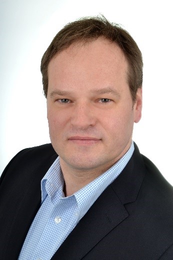 |
Dipl.-Ing. (FH) Axel Lindloff Application Engineer Pre-Sales Koh Young Europe |
| Axel Lindloff studied general electrical engineering at the Bielefeld University of Applied Sciences and has been active in the SMT world since 1999. Since September 2012 Mr. Lindloff has been working for Koh Young Europe GmbH as an application engineer. Here he mainly deals with questions relating to solder paste printing and process optimization with the 3D data obtained. |
Request recording now for free!






.png)




.png)



.png)
